The semiconductor industry confronts a paradox that few anticipated: the limiting factor in AI scaling is no longer algorithmic innovation or training data availability, but rather the physical machines that manufacture chips. ASML's extreme ultraviolet (EUV) lithography systems represent perhaps the most critical technological chokepoint in modern computing infrastructure. These machines enable the sub-5nm process nodes essential for cutting-edge AI accelerators, yet ASML maintains near-total monopolistic control over production. As major foundries and chip designers race to secure capacity for next-generation AI processors, ASML's manufacturing throughput has become the de facto ceiling on computational progress.
This supply constraint arrives at a moment of unprecedented demand acceleration. The exponential scaling laws driving transformer-based models and emerging multimodal architectures depend fundamentally on access to advanced silicon. Companies like NVIDIA, AMD, and custom silicon developers at major cloud providers have collectively signaled that they cannot secure sufficient chip wafer capacity to meet their AI infrastructure roadmaps. ASML's current production rates—delivering approximately 30-40 EUV systems annually—create a compounding bottleneck that threatens to decouple hardware availability from algorithmic progress.
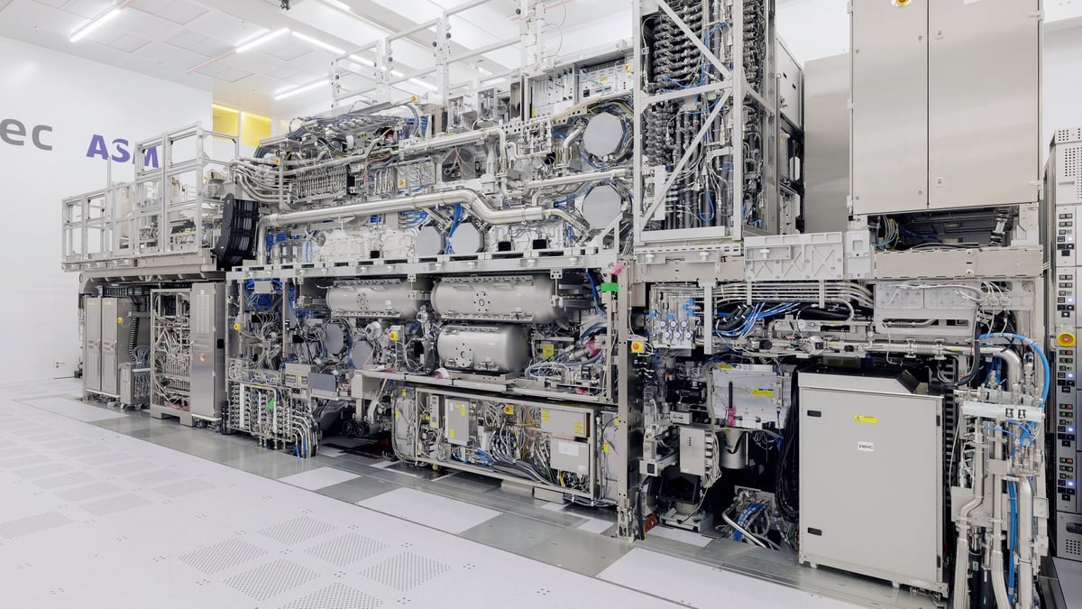
ASML's EUV lithography platform represents perhaps the most complex manufacturing technology ever commercialized. The systems employ laser-generated plasma to produce extreme ultraviolet light at 13.5 nanometers wavelength, enabling patterning of features below 7 nanometers. Each machine requires over 100,000 individual components, incorporates custom optical systems with nanometer-scale precision, and demands cleanroom environments maintaining particle counts below 1 particle per cubic foot. The manufacturing process itself spans 18-24 months per unit, with yield rates that have historically constrained production scaling. The company's Veldhoven headquarters houses the primary assembly and testing facilities, creating a geographic concentration risk that has not escaped the attention of policymakers and strategic planners.
The technical architecture underlying EUV production presents genuine engineering constraints that resist simple acceleration. The laser systems generating plasma require custom CO₂ lasers and complex beam delivery optics. The projection optics employ multi-element reflective systems with surface roughness specifications measured in sub-angstrom tolerances. Quality assurance protocols involve months of metrology and validation before shipment. Unlike software systems where scaling production approaches zero marginal cost, manufacturing additional EUV machines requires proportional increases in skilled labor, precision tooling, and component sourcing. ASML's announced expansion plans target increasing annual production to 60+ systems by 2026-2027, but achieving this requires simultaneous scaling of multiple supply chains and workforce expansion in specialized technical roles.
Within the broader AI infrastructure ecosystem, ASML's capacity constraints intersect with geopolitical considerations and foundry economics. Taiwan Semiconductor Manufacturing Company (TSMC) and Samsung represent the primary customers for advanced EUV systems, and their ability to secure allocation determines which organizations can access cutting-edge process nodes. This creates a secondary market dynamic where chip designers negotiate with foundries for wafer allocation, further amplifying the scarcity premium. The competitive advantage accruing to organizations with secured foundry relationships—particularly OpenAI's partnership infrastructure, Google's custom silicon programs, and Microsoft's strategic foundry agreements—suggests that hardware access itself becomes a differentiating factor in frontier AI capability development.
CuraFeed Take: ASML's monopoly on EUV lithography represents a structural constraint that will likely dominate AI infrastructure discussions throughout 2025-2027. The company faces genuine technical and operational challenges in scaling production beyond 60-70 systems annually without compromising quality or introducing unacceptable yield losses. However, the financial incentives are extraordinary—each EUV system commands pricing exceeding $150-200 million, and demand visibility extends years into the future. What merits close observation: whether ASML's expansion plans materialize on schedule, and whether competitive alternatives (extreme ultraviolet sources from alternative vendors, or next-generation lithography approaches like high-NA EUV) achieve commercialization timelines that could disrupt the current monopoly. For AI researchers and organizations, the practical implication is sobering: your ability to access frontier computational capabilities increasingly depends on ASML's manufacturing roadmap rather than algorithmic innovation alone. This represents a fundamental shift in how AI progress is constrained—from compute-bound to hardware-availability-bound.